The battle for AI hardware supremacy intensifies: NVIDIA GPUs versus Google TPUs, AMD MI300X, Amazon Trainium, and custom ASICs. Which chip truly wins in training, inference, cost, and energy efficiency? We break down everything — architecture, benchmarks, cloud pricing, and future trends.
The AI Chip Market 2026
The global AI chip market is estimated at $91 billion in 2026, with an annual growth rate of 35%. NVIDIA holds ~80% of the GPU market for AI, but alternatives are multiplying. Google TPUs, AMD MI300X, and custom ASICs (Trainium, Maia) are dynamically reshaping the landscape.
GPUs: The Dominant Force in AI
Graphics Processing Units (GPUs) weren't originally designed for AI. They were created for rendering graphics in video games — thousands of small cores executing parallel computations on pixels. But that very parallel processing architecture made them ideal for neural networks.
From Gaming to AI: The NVIDIA Story
- 2006-2007: NVIDIA launches CUDA (Compute Unified Device Architecture), enabling general-purpose computing on GPUs. The beginning of a revolution.
- 2012: AlexNet wins the ImageNet competition using two NVIDIA GTX 580s. Deep learning explodes.
- 2016-2017: Tesla P100 (Pascal) & V100 (Volta) with Tensor Cores — specialized cores for matrix multiplication, 5,120 CUDA cores, 640 Tensor Cores.
- 2020: A100 (Ampere) — 80 GB HBM2e, 312 TFLOPS TF32, MIG (Multi-Instance GPU) for virtualization.
- 2022: H100 (Hopper) — 80 GB HBM3, 989 TFLOPS TF32, Transformer Engine, 3x faster training than A100.
- 2024: B200 (Blackwell) — 192 GB HBM3e, 4,500 TFLOPS FP4, 2nd generation Transformer Engine. Plus GB200 NVL72: 72 B200 GPUs + 36 Grace CPUs in one rack, 20 petaFLOPS at ~$3M.
- 2025: B300/GB300 — Next-gen Blackwell Ultra, 288 GB HBM3e, 10+ petaFLOPS per chip.
"The era of general-purpose computing is over. GPU accelerated computing is the norm."
— Jensen Huang, CEO NVIDIA (GTC 2024)
TPUs: Google's Answer
Tensor Processing Units (TPUs) were created by Google specifically for machine learning workloads — they don't do graphics, they don't do general-purpose computing. They're ASICs (Application-Specific Integrated Circuits), designed exclusively for matrix multiplication, the fundamental operation behind every neural network.
TPU Evolution: 7 Generations in 10 Years
- TPU v1 (2015): First generation, 28nm process, 700 MHz, 8-bit integer, 23 TOPS, 8 GB DDR3. Inference only. Used in AlphaGo vs Lee Sedol (2016).
- TPU v2 (2017): 16nm, 16 GB HBM, 45 TFLOPS, bfloat16 format — first time both training + inference. Pods: 256 chips, 11.5 petaFLOPS.
- TPU v3 (2018): 32 GB HBM, 123 TFLOPS, liquid cooling. Pods: 1,024 chips, 100+ petaFLOPS.
- TPU v4 (2021): 7nm, 275 TFLOPS bf16, 32 GB HBM, optically reconfigurable interconnect. Google claims 5-87% faster than NVIDIA A100 on ML benchmarks.
- TPU v5p (2023): 459 TFLOPS bf16, 95 GB HBM, 2,765 GB/s bandwidth — competitive with H100.
- TPU v6e Trillium (2024): 918 TFLOPS bf16, 4.7x performance increase vs v5e, 32 GB HBM.
- TPU v7 Ironwood (April 2025): 4,614 TFLOPS FP8, 192 GB HBM, 7.37 TB/s bandwidth, energy efficiency 4.7 TOPS/W. Pods: 9,216 chips.
Important to note: TPUs are designed in-house but manufactured in partnership with Broadcom, which provides SerDes interfaces and manages fabrication through TSMC. Since September 2025, Google has been in talks with neoclouds (Crusoe, CoreWeave) and even Meta about deploying TPUs.
Architectural Differences: GPU vs TPU
Fundamental Differences
GPU (NVIDIA): SIMT architecture (Single Instruction, Multiple Threads). Thousands of small cores (16,896 CUDA cores on H100) + specialized Tensor Cores. General-purpose — supports gaming, scientific computing, visualization AND AI.
TPU (Google): Systolic array architecture. Large matrix multiplication units in silicon, optimized for matrix multiplication. ASIC — does ONLY machine learning. No rendering, no CUDA support.
The Practical Implications
- Flexibility: GPUs run virtually every framework (PyTorch, TensorFlow, JAX, ONNX). TPUs support TensorFlow, JAX, and now PyTorch — but with limited optimization.
- Precision: GPUs support FP64/FP32/FP16/BF16/FP8/INT8. TPUs focus on BF16/INT8 — sufficient for ML but not for scientific computing.
- Memory: H100: 80 GB HBM3 (3.35 TB/s). B200: 192 GB HBM3e (8 TB/s). TPU v7 Ironwood: 192 GB HBM (7.37 TB/s). Practically equivalent.
- Interconnect: NVIDIA NVLink/NVSwitch (900 GB/s per GPU). Google ICI (Inter-Chip Interconnect) with optical connections on TPU v4+.
Head-to-Head: Training vs Inference
AI Training
For training large models (LLMs, vision models), NVIDIA GPUs dominate in raw power. The GB200 NVL72 rack unit delivers 20 petaFLOPS in a single rack. But TPUs excel in cost efficiency on Google Cloud — especially for JAX-based workloads.
- Speed: NVIDIA B200 ≈ 4,500 TFLOPS FP4 vs TPU v7 ≈ 4,614 TFLOPS FP8. Nearly equivalent in raw performance.
- Ecosystem: 90%+ of researchers use CUDA + PyTorch. Switching to TPU means changing the entire software stack.
- Scaling: TPU pods up to 9,216 chips vs NVIDIA DGX SuperPOD (1,024+ GPUs). TPUs were designed from the start for massive scaling.
AI Inference
For inference — where models “run” in production — energy efficiency becomes critical. TPU v7 Ironwood achieves 4.7 TOPS/W — an impressive figure. Google uses TPUs for Google Search, Gmail, Google Photos, YouTube recommendations, and of course Gemini.
The Other Players
- AMD MI300X: 192 GB HBM3, 1,300 TFLOPS FP16. AMD targets pricing ~20-30% lower than NVIDIA H100. Open-source ROCm stack — improving but still far behind in ecosystem.
- Amazon Trainium2: Custom ASIC on AWS. Up to 100,000 chips in UltraClusters. Designed for Llama, GPT-style training. Cost 30-50% lower than equivalent NVIDIA instances.
- Microsoft Maia 100: Custom AI chip, 5nm TSMC. Used internally in Azure for Copilot/Bing AI. Liquid cooling, 820+ TFLOPS.
- Intel Gaudi 3: 1,835 TFLOPS BF16, 128 GB HBM2e. Intel claims 50% better perf/$ than H100 for inference.
- Groq LPU: Language Processing Unit — TSP architecture, designed SOLELY for inference. Extremely low latency, ~500 tokens/sec on Llama 3.
The Cost Battle: Cloud Pricing 2026
For most companies, the GPU vs TPU comparison is practically a cloud pricing comparison:
Cloud Costs (On-Demand, per hour)
NVIDIA A100 80GB: AWS p4d.24xlarge ~$32/hr (8 A100s) | GCP a2-ultragpu-8g ~$29/hr
NVIDIA H100 80GB: AWS p5.48xlarge ~$98/hr (8 H100s) | GCP a3-megagpu-8g ~$87/hr
Google TPU v5p: GCP ~$4.20/hr per chip (8-chip pod ~$34/hr)
Google TPU v6e: GCP ~$3.22-$6.44/hr per chip
AWS Trainium2: trn2.48xlarge ~$24/hr (16 chips)
AMD MI300X: AWS p5e ~$76/hr (8 MI300X)
In raw $/TFLOPS, TPUs tend to be more economical — but only if your workload runs well on JAX or optimized TensorFlow. Porting a PyTorch codebase to TPU can cost weeks or months of engineering.
When to Choose GPU vs TPU
- Choose NVIDIA GPU if: You use PyTorch, need flexibility (training + inference + R&D), want a massive ecosystem, or run specialized workloads (3D rendering, scientific simulation + AI).
- Choose Google TPU if: You work with JAX/TensorFlow, run massive-scale training on Google Cloud, prioritize cost efficiency, or build inference pipelines for production services.
- Consider AMD MI300X if: You want an NVIDIA alternative at lower price, your workload doesn't need bleeding-edge CUDA features, or you work in open-source ecosystems.
- Consider Trainium/Inferentia if: You work exclusively on AWS, want maximum cost savings, and your model is supported (Llama, Stable Diffusion, etc.).
The Future: 2026 and Beyond
The battle intensifies on every front:
- NVIDIA Rubin (2026): The next architecture, with HBM4 memory, aims for 10x+ performance/watt vs Hopper. Jensen Huang promised “a new chip every year.”
- Google TPU v8: Expected 2026-2027 with possible 3nm process, even greater energy efficiency.
- ARM-based AI Chips: NVIDIA's Grace-Blackwell architecture unites ARM CPU + GPU. Apple M4 Ultra with its 32-core Neural Engine shows the ARM/AI convergence is accelerating.
- Photonic/Optical Computing: Startups like Lightmatter are developing photon-based AI chips — potentially 100x more energy efficient.
- Chiplet Architecture: Instead of a single monolithic die, smaller chiplets connect together (AMD MI300X already uses chiplets). Enables higher yields and mix-and-match designs.
"TPUs achieved 15-30x higher performance and 30-80x higher performance-per-watt than contemporary CPUs and GPUs."
— Norman Jouppi et al., ISCA 2017 (Google TPU paper)
Verdict: Which One Wins?
The honest answer: it depends. There is no absolute winner.
- Ecosystem & Flexibility: NVIDIA GPU wins — nobody's going to surpass the CUDA ecosystem built over 18 years.
- Cost Efficiency (at scale): TPU wins — especially for Google Cloud workloads with JAX.
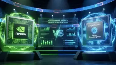
- Raw Performance: Tie — TPU v7 Ironwood (4,614 TFLOPS) vs NVIDIA B200 (4,500 TFLOPS) are practically equivalent.
- Inference at Scale: TPU wins — Google runs Gemini, Search, and YouTube recommendations on TPUs.
- Availability: NVIDIA GPU wins — available on every cloud provider, every data center, every lab.
Ultimately, the question “GPU or TPU?” is gradually being replaced by “what hardware mix do I need?” The biggest players (Google, Meta, Microsoft, Amazon) use both — or build their own custom chips. The future of AI compute isn't one chip, but an entire ecosystem.